mmWave Materials and Test
Topic Chair: Dr. Urmi Ray, INEMI
Contributing organizations: INEMI, Intel, NIST, QWED, Keysight Technologies
Acknowledgement
As part of the 5G/6G MAESTRO project, work on this topic (“mmWave Materials and Test”) and its child pages, is supported by the Office of Advanced Manufacturing in the National Institute of Standards and Technology (NIST), under the Federal Award ID Number 70NANB22H050.
Scope
This topic considers the challenges posed by the operation of electronics at mmWave frequencies and higher. The focus is on the materials, their characterization and electrical test, all primarily for PCBs and packaging substrates.
Materials Development
Multiple challenges exist in ensuring the cost-effective availability of materials used in hardware used in millimeter wave frequencies (5G, 6G and beyond). That includes the integrated circuits (IC) used in the transceiver or modem, the substrates used for packaging the ICs and printed circuit boards and the overall hardware solutions.
Material performance in terms of losses is a key determinant for the level of coverage and penetration achieved by a mobile cellular system: Lower loss materials for improved system link budgets
The figure below provides qualitative comparison of various materials considered for 5G hardware.
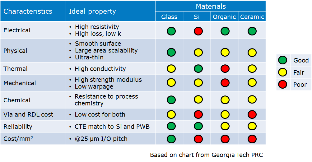
Figure 1. Qualitative properties of materials for 5G hardware
Other materials used in 5G semiconductor packaging include:
New substrates, such as glass or fused silica for improved RF performance
Package substrate/PCB core material
Solder resist/underfill
Mold Material
Technical Drivers
Lower loss materials for improved system link budgets will be crucial for the success of affordable mmWave systems.
Critical materials parameters that affect the overall electrical properties of mmWave hardware are as follows:
Low-Loss Dielectric Materials Characterization
Circuit designers need dielectric property data for materials at millimeter-wave (mmWave) frequencies to optimize device performance of new hardware and for quality assurance. However, there are no standard traceable reference materials or even agreed upon characterization test methods for materials at mmWave frequencies. Further, at higher frequencies, smaller test samples are required, placing more stringent limits on the allowable dimensional variations in those samples. Without reliable mmWave materials data, manufacturers are forced to extrapolate materials data from low frequencies to high frequencies, which can lead to mistakes that have potentially devastating costs.
A detailed view of the needs, gaps, challenges and technology solutions for this topic is given here.
Electrical Test
Electrical testing at high frequencies (particularly at mmWave) is a challenge, both from a technical perspective, as well as scaling up to high volume production. With the advent of mmWave communications, smartphone architectures need new test strategies, due to the higher port counts, the extensive use of signal beamforming and the introduction of antenna-in-package (AIP) technologies.
The test challenges impact both wafer level (IC level) to package level (ATE - Automated Test Equipment) and system level test (SLT).
High-volume silicon chips bring mmWave testing into the ATE world for the first time. However, due to lack of agreement amongst various players, and also lack of standardization, multiple implementation strategies are being developed.
Your Feedback
We welcome your comments and suggestions! Here is a link for your input.
As part of the 5G/6G MAESTRO project, work on this page is supported by the Office of Advanced Manufacturing in the National Institute of Standards and Technology (NIST), under the Federal Award ID Number 70NANB22H050.